
Author Affiliations
Abstract
1 Jinan University, College of Physics & Optoelectronic Engineering, Institute of Nanophotonics, Guangdong Provincial Key Laboratory of Nanophotonic Manipulation, Guangzhou, China
2 Tsinghua University, Shenzhen International Graduate School, State Key Laboratory of Chemical Oncogenomics, Shenzhen, China
3 Jinan University, College of Life Science and Technology, Guangzhou, China
Narrowband photodetection is an important measurement technique for material analysis and sensing, for example, nondispersive infrared sensing technique. Both photoactive material engineering and nanophotonic filtering schemes have been explored to realize wavelength-selective photodetection, while most devices have a responsive bandwidth larger than 2% of the operating wavelength, limiting sensing performance. Near-infrared photodetection with a bandwidth of less than 0.2% of the operating wavelength was demonstrated experimentally in Au/Si Schottky nanojunctions. A minimum linewidth of photoelectric response down to 2.6 nm was obtained at a wavelength of 1550 nm by carefully tailing the absorptive and radiative loss in the nanostructures. Multiple functions were achieved on chip with the corrugated Au film, including narrowband resonance, light harvesting for sensing and photodetection, and electrodes for hot electron emission. Benefiting from such a unity integration with in situ photoelectric conversion of the optical sensing signal and the ultranarrowband resonance, self-contained on-chip biosensing via simple intensity interrogation was demonstrated with a limit of detection down to 0.0047% in concentration for glucose solution and 150 ng / mL for rabbit IgG. Promising potential of this technique is expected for the applications in on-site sensing, spectroscopy, spectral imaging, etc.
plasmonics hot electron sensor photodetector spectroscopy Advanced Photonics
2024, 6(2): 026007

Author Affiliations
Abstract
1 Institute of Nanophotonics, Jinan University, Guangzhou 511443, China
2 Hangzhou Dianzi University, Hangzhou 310018, China
3 James Watt School of Engineering, University of Glasgow, Glasgow G12 8QQ, UK
Epsilon-near-zero (ENZ) modes have attracted extensive interests due to its ultrasmall mode volume resulting in extremely strong light-matter interaction (LMI) for active optoelectronic devices. The ENZ modes can be electrically toggled between on and off states with a classic metal-insulator-semiconductor (MIS) configuration and therefore allow access to electro-absorption (E-A) modulation. Relying on the quantum confinement of charge-carriers in the doped semiconductor, the fundamental limitation of achieving high modulation efficiency with MIS junction is that only a nanometer-thin ENZ confinement layer can contribute to the strength of E-A. Further, for the ENZ based spatial light modulation, the requirement of resonant coupling inevitably leads to small absolute modulation depth and limited spectral bandwidth as restricted by the properties of the plasmonic or high-Q resonance systems. In this paper, we proposed and demonstrated a dual-ENZ mode scheme for spatial light modulation with a TCOs/dielectric/silicon nanotrench configuration for the first time. Such a SIS junction can build up two distinct ENZ layers arising from the induced charge-carriers of opposite polarities adjacent to both faces of the dielectric layer. The non-resonant and low-loss deep nanotrench framework allows the free space light to be modulated efficiently via interaction of dual ENZ modes in an elongated manner. Our theoretical and experimental studies reveal that the dual ENZ mode scheme in the SIS configuration leverages the large modulation depth, extended spectral bandwidth together with high speed switching, thus holding great promise for achieving electrically addressed spatial light modulation in near- to mid-infrared regions. Epsilon-near-zero (ENZ) modes have attracted extensive interests due to its ultrasmall mode volume resulting in extremely strong light-matter interaction (LMI) for active optoelectronic devices. The ENZ modes can be electrically toggled between on and off states with a classic metal-insulator-semiconductor (MIS) configuration and therefore allow access to electro-absorption (E-A) modulation. Relying on the quantum confinement of charge-carriers in the doped semiconductor, the fundamental limitation of achieving high modulation efficiency with MIS junction is that only a nanometer-thin ENZ confinement layer can contribute to the strength of E-A. Further, for the ENZ based spatial light modulation, the requirement of resonant coupling inevitably leads to small absolute modulation depth and limited spectral bandwidth as restricted by the properties of the plasmonic or high-Q resonance systems. In this paper, we proposed and demonstrated a dual-ENZ mode scheme for spatial light modulation with a TCOs/dielectric/silicon nanotrench configuration for the first time. Such a SIS junction can build up two distinct ENZ layers arising from the induced charge-carriers of opposite polarities adjacent to both faces of the dielectric layer. The non-resonant and low-loss deep nanotrench framework allows the free space light to be modulated efficiently via interaction of dual ENZ modes in an elongated manner. Our theoretical and experimental studies reveal that the dual ENZ mode scheme in the SIS configuration leverages the large modulation depth, extended spectral bandwidth together with high speed switching, thus holding great promise for achieving electrically addressed spatial light modulation in near- to mid-infrared regions.
epsilon-near-zero modulation TCOs electro-optic light harvesting Opto-Electronic Advances
2022, 5(6): 200093
红外与激光工程
2022, 51(1): 20210671
暨南大学纳米光子学研究院,广东 广州 510632
光谱分析技术具有快速、准确和绿色检测的特点,在科学研究、信息、生物医疗、食药检测、农业、环境和安防等领域有广泛而且重要的应用。然而现有光谱技术与检测设备通常较为庞大复杂,难以适合现场快检、轻载荷平台等便携式应用场景。近年来,微型光谱检测技术和设备受到广泛关注并得到迅速发展,具有尺寸、重量、功耗等方面的显著优势,尤其是基于散斑检测的计算光谱分析技术,可以通过记录分析散射元件对被测光形成的散斑图获得高精度的光谱信息。本文将介绍相关技术原理和技术发展现状,分析现有技术性能和优缺点,讨论并总结未来发展方向和应用前景。
光谱 散斑 微型光谱仪 压缩感知 spectrum speckle microspectrometer compressive sensing
暨南大学纳米光子学研究院, 广东 广州 511443
近年来,各种微纳光学效应被用于实现结构色甚至更精细的光谱调控,但这类方法大部分都基于彩色滤波原理,其光学效率难以接近甚至超越传统的染料滤波技术。首先介绍高像素密度图像传感器的色彩技术需求,并分析现有商用染料滤波器和微纳光学结构色滤波技术的局限性,然后介绍一类新兴的微纳结构空间分光色彩管理技术,并系统性地分析和讨论其技术原理和发展现状,最后总结该技术面临的挑战和发展趋势。
光学器件 亚波长结构 微纳光学 图像传感器 结构色 分束器
Author Affiliations
Abstract
1 Shanghai Institute of Technical Physics, Chinese Academy of Sciences, Shanghai 200083, P. R. China
2 State Key Laboratory of Infrared Physics, Shanghai Institute of Technical Physics, Chinese Academy of Sciences, Shanghai 200083, P. R. China
3 School of Physical Science and Technology, ShanghaiTech University, Shanghai 201210, P. R. China
4 Institute of Photomedicine, Shanghai Skin Disease Hospital, Tongji University School of Medicine, Shanghai 200071, P. R. China
5 Department of Gerontology, Xinhua Hospital, Shanghai Jiaotong University, Shanghai 200092, P. R. China
Fluorescence imaging is very useful for skin cancer lesions detection because of its properties of noninvasion and fast imaging. However, conventional fluorescence imaging devices' excitation light source and camera are usually separated, which will cause problems such as complicated structure, large volume, and poor illumination homogeneity. In this paper, we introduce a miniature portable fluorescence imaging device to diagnose skin cancer. A coaxial design has been introduced to combine the exciting light source and fluorescence receiver as an integral part, which significantly reduces the size of the device and ensures illumination homogeneity. The volume of the device is less than 3.5 × 3.5 × 9.5 cm3 with weight of 150 g, and the total power (including the excitation lamp) is only 1.5 W. It is used to detect the squamous cell carcinoma mice for demonstration. The results show that the location of the cancer lesions can be easily distinguished from the images captured by the device. It can be efficiently used to detect early skin tumors with noninvasion. It also has prospects to be integrated with other diagnostic methods such as ultrasound probe, for multiple diagnose of skin tumors thanks to its miniature size.
Protoporphyrin IX coaxial design skin cancer Journal of Innovative Optical Health Sciences
2021, 14(2): 2050026
暨南大学纳米光子学研究院, 广东 广州 510632
近年来,表面等离激元(SP)增强的金属纳米结构中热载流子产生、传输和收集得到了广泛而深入的研究。其中,利用电子隧穿和热发射效应实现的全新光电转换机制,结合平面化制作和CMOS兼容集成等,有望成为硅基红外光电探测的备选方案。目前这类探测器主要为金属-半导体肖特基结的光伏型器件,其光电响应较弱。为此,报道了一种基于金属-硅复合无序纳米结构的光电导器件,得益于无序表面等离激元局域热点效应和多叉指金属-半导体-金属(MSM)结构的显著光电导增益,实验获得了硅亚带隙的宽带强光电响应。该热载流子介导的多叉指MSM器件在1310 nm波长处的光电流响应度高达2.50 A/W。
探测器 近红外探测器 光电导探测器 等离激元 光电导增益 中国激光
2020, 47(11): 1113002
Author Affiliations
Abstract
1 Institute of Nanophotonics, Jinan University, Guangzhou 511443, China
2 University of Electronic Science and Technology of China, Chengdu 610054, China
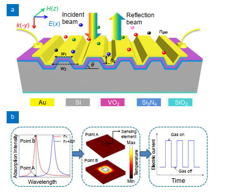
Gas identification and concentration measurements are important for both understanding and monitoring a variety of phenomena from industrial processes to environmental change. Here a novel mid-IR plasmonic gas sensor with on-chip direct readout is proposed based on unity integration of narrowband spectral response, localized field enhancement and thermal detection. A systematic investigation consisting of both optical and thermal simulations for gas sensing is presented for the first time in three sensing modes including refractive index sensing, absorption sensing and spectroscopy, respectively. It is found that a detection limit less than 100 ppm for CO2 could be realized by a combination of surface plasmon resonance enhancement and metal-organic framework gas enrichment with an enhancement factor over 8000 in an ultracompact optical interaction length of only several microns. Moreover, on-chip spectroscopy is demonstrated with the compressive sensing algorithm via a narrowband plasmonic sensor array. An array of 80 such sensors with an average resonance linewidth of 10 nm reconstructs the CO2 molecular absorption spectrum with the estimated resolution of approximately 0.01 nm far beyond the state-of-the-art spectrometer. The novel device design and analytical method are expected to provide a promising technique for extensive applications of distributed or portable mid-IR gas sensor.
gas sensor mid-IR on-chip surface plasmon resonance spectroscopy Opto-Electronic Advances
2020, 3(7): 07190040
1 上海市激光技术研究所, 上海 200233
2 上海激光直接物标溯源工程技术研究中心, 上海 200233
3 同济大学医学院上海市皮肤病医院光医学研究所, 上海 200443
4 上海仪器仪表研究所, 上海 200063
研制了一种小型化便携式的激光诱导荧光的检测系统。检测系统 以 405 nm的稳谱半导体激光器作为激光光源, 荧光光纤探头和光纤作为荧光的收集系统, 光栅光谱仪作为荧光分析装置, 采集和分析经过5-氨基酮戊酸(ALA))处理后的鳞癌小鼠模型的原卟啉IX的荧光光谱, 对皮肤癌开展光动力学荧光诊断的初步实验研究。
激光诱导荧光 荧光检测 5-氨基酮戊酸 光动力学荧光诊断 laser-induced fluorescence fluorescence detecting ALA photodynamic fluorescence diagnosis
1 中国科学院苏州纳米技术与纳米仿生研究院 中国科学院纳米器件与应用重点实验室, 江苏 苏州215123
2 中国科学技术大学 纳米技术与纳米仿生学院, 安徽 合肥 230026
3 暨南大学 纳米光子学研究院 广东省光纤传感与通信技术重点实验室, 广东 广州511443
近年来, 太赫兹技术得到迅速发展, 在通信、反恐、检测和医药等领域展现了广泛的应用潜力。尤其是许多生物分子和材料在太赫兹波段存在特征的吸收光谱, 而且太赫兹波能量低损伤小等特点, 使得太赫兹生化传感器越来越受到关注。然而, 由于太赫兹波的波长较长与生物分子等的尺寸差别非常大, 导致相互作用比较弱, 从而限制了太赫兹传感器的性能。通过微纳电磁结构对光场空间分布和频率分布的调控, 增强太赫兹波传感器的灵敏度是当前的研究热点。文中将重点介绍各种微纳结构太赫兹传感技术的原理和研究现状, 并通过梳理其发展趋势和当前的性能制约因素, 讨论此方向将来的发展方向和应用前景。
太赫兹 传感器 人工微结构 超材料 terahertz sensor microstructure metamaterial 红外与激光工程
2019, 48(2): 0203001


